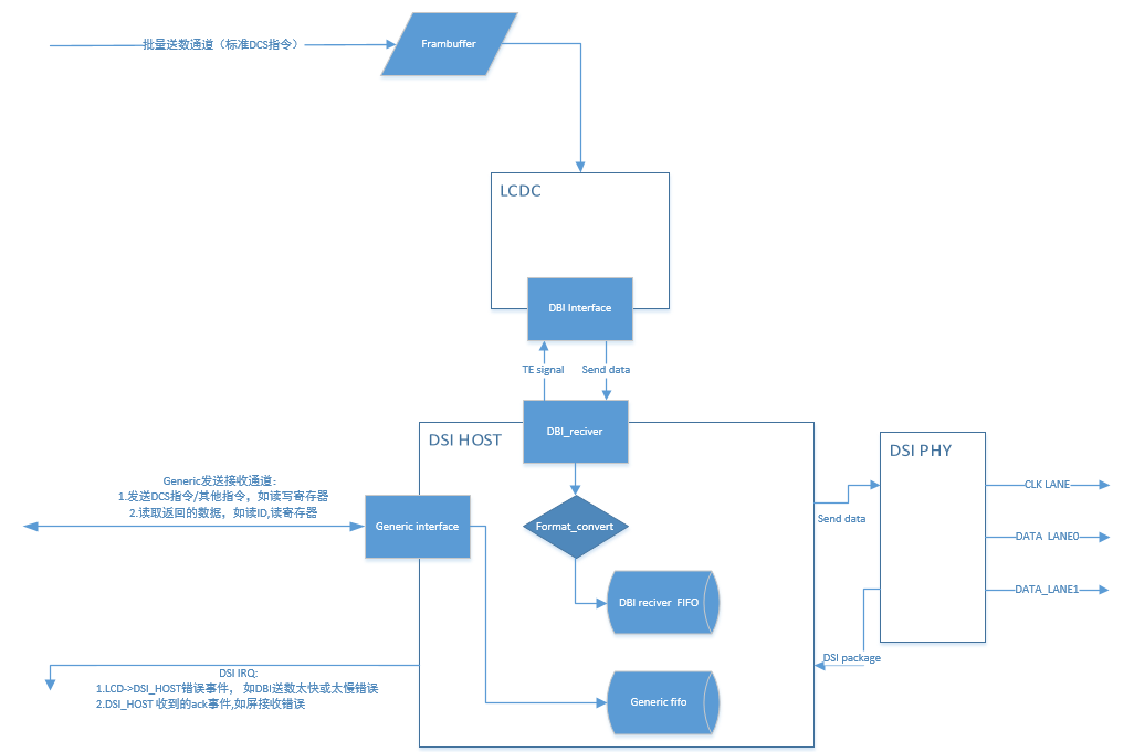
DSI
DSI (MIPI DSI) 模块支持1-lane或者2-lane的DSI屏幕, 目前带宽支持240/288/336/384/480Mbps几种配置, 标准参考MIPI协议版本V1.1(55x不支持Video模式)
支持的颜色输出格式
RGB565 DSI送数时顺序:[G3~G5R0~R4][B0~B4G0~G2]RGB888 DSI送数时顺序:[R0~R7][G0~G7][B0~B7]RGB565_SWAP DSI送数时顺序(55X 不支持):[B0~B4G0~G2][G3~G5R0~R4]
DSI 模块可以独立工作, 但是通过LCDC封装的接口来操作可以达到最优性能。
备注
在55x上 DSI需要分多次才能完成整个屏幕的刷新动作,每次刷新2N行(视刷新区域大小,N会不同), 直到完成整个屏幕的刷新
使用DSI示例
通过LCDC接口打开DSI屏幕,然后画一个100x100的矩形区域到LCD的操作:
static LCDC_HandleTypeDef hlcdc_rm69090;


/*DSI LCD configuration*/
static const LCDC_InitTypeDef lcdc_int_cfg =
{
    .lcd_itf = LCDC_INTF_DSI,                              //LCDC output interface
    .freq = DSI_FREQ_288MHZ,                               //DSI clk lane freqence(DDR freqence)
    .color_mode = LCDC_PIXEL_FORMAT_RGB888,                //LCDC DBI output color format, should match with CmdCfg.ColorCoding below

    .cfg = {

        .dsi = {

            .Init = {
                .AutomaticClockLaneControl = DSI_AUTO_CLK_LANE_CTRL_DISABLE,        //Auto gate clock to save power
                .NumberOfLanes = DSI_TWO_DATA_LANES,                                //Numbers of data-lane
                .TXEscapeCkdiv = 0x2,                                               //Escape clk = lcdc_int_cfg_dsi.freq / 2 / 8 / TXEscapeCkdiv
            },

            .CmdCfg = {
                .VirtualChannelID      = 0,                             //Fixed 0,  DBI virtual channel id
                .CommandSize           = 0xFFFF,                        //Maximum write bytes of every partial write
                .TEAcknowledgeRequest  = DSI_TE_ACKNOWLEDGE_ENABLE,     //Open or Close TE
                .ColorCoding           = DSI_RGB888,                    //DSI-DBI input color format and DSI output format
            },

            .PhyTimings = { /*DSI PHY config */
                .ClockLaneHS2LPTime = 35,  /* The maximum time that the D-PHY clock lane takes to go from high-speed
                                              to low-power transmission                                              */
                .ClockLaneLP2HSTime = 35,  /* The maximum time that the D-PHY clock lane takes to go from low-power
                                              to high-speed transmission                                             */
                .DataLaneHS2LPTime = 35,   /* The maximum time that the D-PHY data lanes takes to go from high-speed
                                              to low-power transmission                                              */
                .DataLaneLP2HSTime = 35,   /* The maximum time that the D-PHY data lanes takes to go from low-power
                                              to high-speed transmission                                             */

                .DataLaneMaxReadTime = 0,  /* The maximum time required to perform a read command */
                .StopWaitTime = 10,        /* The minimum wait period to request a High-Speed transmission after the
                                              Stop state                                                             */
            },

            .HostTimeouts = {
                .TimeoutCkdiv = 1,                          //Timeout clk = lcdc_int_cfg_dsi.freq / 2 / 8 / TimeoutCkdiv
                .HighSpeedTransmissionTimeout = 0,
                .LowPowerReceptionTimeout = 0,
                .HighSpeedReadTimeout = 0,
                .LowPowerReadTimeout = 0,
                .HighSpeedWriteTimeout = 0,
                //.HighSpeedWritePrespMode = DSI_HS_PM_DISABLE,
                .LowPowerWriteTimeout = 0,
                .BTATimeout = 0,
            },


            .LPCmd = {
                .LPGenShortWriteNoP    = DSI_LP_GSW0P_ENABLE,     //Generic short write 0 parameter use LP mode
                .LPGenShortWriteOneP   = DSI_LP_GSW1P_ENABLE,     //Generic short write 1 parameter use LP mode
                .LPGenShortWriteTwoP   = DSI_LP_GSW2P_ENABLE,     //Generic short write 2 parameter use LP mode
                .LPGenShortReadNoP     = DSI_LP_GSR0P_ENABLE,     //Generic short read 0 parameter use LP mode
                .LPGenShortReadOneP    = DSI_LP_GSR1P_ENABLE,     //Generic short read 0 parameter use LP mode
                .LPGenShortReadTwoP    = DSI_LP_GSR2P_ENABLE,     //Generic short read 0 parameter use LP mode
                .LPGenLongWrite        = DSI_LP_GLW_ENABLE,       //Generic long write use LP mode
                .LPDcsShortWriteNoP    = DSI_LP_DSW0P_ENABLE,     //Dcs short write 0 parameter use LP mode
                .LPDcsShortWriteOneP   = DSI_LP_DSW1P_ENABLE,     //Dcs short write 1 parameter use LP mode
                .LPDcsShortReadNoP     = DSI_LP_DSR0P_ENABLE,     //Dcs short read 0 parameter use LP mode
                .LPDcsLongWrite        = DSI_LP_DLW_DISABLE,      //Dcs long write use HS mode
                .LPMaxReadPacket       = DSI_LP_MRDP_ENABLE,      //Maximum Read Packet Size
                .AcknowledgeRequest    = DSI_ACKNOWLEDGE_DISABLE, //Request acknowledge
            },


            .vsyn_delay_us = 1000,  //The delay during receive TE and send framebuffer. If TE was disable ignore it.
        },
    },
};


/**********************
 *   FUNCTIONS
 **********************/

__ROM_USED void LCDC1_IRQHandler(void)
{
    /* enter interrupt */
    ENTER_INTERRUPT();

    HAL_LCDC_IRQHandler(&hlcdc_rm69090);

    /* leave interrupt */
    LEAVE_INTERRUPT();
}


void HAL_LCDC_SendLayerDataCpltCbk(LCDC_HandleTypeDef *lcdc)
{
    LOG_I("Send layer buffer done.");
}

/*
    RM69090 initialization sequence
 */
static void RM69090_Init_Seq(LCDC_HandleTypeDef *hlcdc)
{
    ...

    //Sleep out
    HAL_LCDC_WriteU8Reg(hlcdc, 0x11, (uint8_t *)NULL, 0);

    /* Wait for 150ms */
    HAL_Delay(150);

    /* Display On */
    HAL_LCDC_WriteU8Reg(hlcdc, 0x29, (uint8_t *)NULL, 0);

    /* Wait for 150ms */
    HAL_Delay(150);

    ...
}


/*Set LCD receive area*/
void RM69090_SetRegion(LCDC_HandleTypeDef *hlcdc, uint16_t x0, uint16_t y0, uint16_t x1, uint16_t y1)
{
    uint8_t   parameter[4];

    parameter[0] = (x0) >> 8;
    parameter[1] = (x0) & 0xFF;
    parameter[2] = (x1) >> 8;
    parameter[3] = (x1) & 0xFF;
    HAL_LCDC_WriteU8Reg(hlcdc, 0x2a, parameter, 4);

    parameter[0] = (y0) >> 8;
    parameter[1] = (y0) & 0xFF;
    parameter[2] = (y1) >> 8;
    parameter[3] = (y1) & 0xFF;
    HAL_LCDC_WriteU8Reg(hlcdc, 0x2b, parameter, 4);
}


static void main(int argc, char **argv)
{
    uint8_t *p_framebuffer = (uint8_t *) 0x60020000;

    /*Turn on LCD board power supply*/
    Poweron_LCD_Board();


    memset(&hlcdc_rm69090, 0, sizeof(hlcdc_rm69090));

    hlcdc_rm69090.Instance = hwp_lcdc;

    /*Set background layer color*/
    hlcdc_rm69090.bg.r = 0;
    hlcdc_rm69090.bg.g = 0;
    hlcdc_rm69090.bg.b = 255;

    /*Set default layer configuration*/
    hlcdc_rm69090.Layer.layer_alpha_en = 0;
    hlcdc_rm69090.Layer.alpha = 255;
    hlcdc_rm69090.Layer.chroma_key_en = 0;

    memcpy(&hlcdc_rm69090.Init, &lcdc_int_cfg, sizeof(LCDC_InitTypeDef));

    /*Open DSI & LCDC */
    HAL_LCDC_Init(&hlcdc_rm69090);

    /*  Reset LCD by RESX pin */
    HAL_LCDC_ResetLCD(&hlcdc_rm69090, LCDC_RESX_NEG_PULSE, 20);
    /* Wait for 200ms */
    HAL_Delay(200);


    /*DSI LCD initial */
    RM69090_Init_Seq(&hlcdc_rm69090);

    {//Read LCD id

        uint32_t rd_data = 0;

        HAL_LCDC_ReadU8Reg(&hlcdc_rm69090, 0x04, (uint8_t *)&rd_data, 4);
        LOG_I("rm69090 id is %d",rd_data);
    }

    /*Disable layer compress*/
    HAL_LCDC_LayerSetCmpr(&hlcdc_rm69090, HAL_LCDC_LAYER_DEFAULT, 0);
    /*Set layer format RGB565*/
    HAL_LCDC_LayerSetFormat(&hlcdc_rm69090, HAL_LCDC_LAYER_DEFAULT,LCDC_PIXEL_FORMAT_RGB565);

    /*Fill frambuffer with single color*/
    memset(p_framebuffer, 0xE0, 100*100*2);

    /*Assign framebuffer  and area to layer*/
    HAL_LCDC_LayerSetData(&hlcdc_rm69090, HAL_LCDC_LAYER_DEFAULT, (uint8_t *)p_framebuffer, 100, 100, 199, 199);


    /*Set clip area of all LCDC layer*/
    HAL_LCDC_SetROIArea(&hlcdc_rm69090, 100, 100, 199, 199);

    /*Set LCD receive area */
    RM69090_SetRegion(&hlcdc_rm69090, 100, 100, 199, 199);

    /*Enable LCDC IRQ*/
    HAL_NVIC_SetPriority(LCDC_IRQ_NUM, 3, 0);
    HAL_NVIC_EnableIRQ(LCDC_IRQ_NUM);


    /*
        Start partial writting framebuffer,

       RM69090_SetRegion is the function of setting LCD recieve area, and it was called during partial write DSI LCD
    */
    HAL_LCDC_DSI_StartPatialWrite(&hlcdc_rm69090, 0x2c, (SetRegion_cb_t)RM69090_SetRegion);

    /* Wait for 150ms */
    HAL_Delay(150);

   /*Writing framebuffer is done while LCDC_IRQHandler come*/

    /*Disable LCDC IRQ*/
    HAL_NVIC_DisableIRQ(LCDC_IRQ_NUM);

}