Low Power Development Guide
1 Introduction
SiFli MCUs are dual‑core Cortex‑M33 STAR SoCs. The high‑performance core (HCPU) runs at 0–240 MHz and belongs to the HPSYS subsystem, suitable for graphics, audio, neural networks, and other compute‑intensive workloads. The low‑power core (LCPU) runs at 0–48 MHz and belongs to the LPSYS subsystem, suitable for Bluetooth, sensor data collection, and processing tasks.
Refer to the low‑power example at example\pm\classical.
2 Configure Low‑Power Mode
2.1 Enable Low‑Power Mode
Run sdk.py menuconfig in the project directory to open the configuration menu:
Enable low‑power support (
Enable Low power support):Path: Sifli middleware → Enable Low power support
Toggle: Enable Low power support
Macro:
BSP_USING_PMPurpose: Enable low‑power features
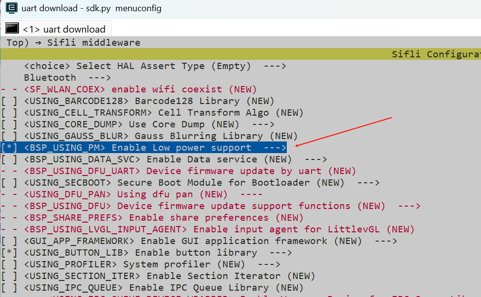
Figure: Enable Low Power configuration menu
Select low‑power mode (
Enable Deep Mode):Path: RTOS → RT‑Thread Components → Device Drivers → Using Power Management device drivers → Select PM Mode
Select: Enable Deep Mode
Macro:
PM_DEEP_ENABLEPurpose: Use Deep Sleep mode as the low‑power mode
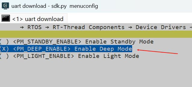
Figure: Deep Sleep configuration menu
Enable PM debug to print low‑power logs (optional; printing logs consumes time and affects power) (
Enable PM Debug):Path: Sifli middleware → Enable Low power support → Enable PM Debug
Select: Enable PM Debug
Macro:
BSP_PM_DEBUGPurpose: Enable low‑power debug logging
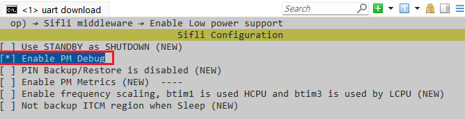
Figure: PM debug configuration menu
After configuration, verify
rtconfig.hincludes the following:
#define RT_USING_PM 1           // Enable PM module
#define PM_DEEP_ENABLE 1        // Use DEEP sleep mode
#define BSP_USING_PM 1          // Enable PM module
#define BSP_PM_DEBUG 1          // Print PM[S], PM[W] logs (optional)
2.2 Disable Low‑Power Mode
Run sdk.py menuconfig and uncheck the same options used to enable low power.
4 Low‑Power Debugging Methods
4.1 Low‑Power Modes
PM_SLEEP_MODE_IDLE: CPU enters idle (WFI/WFE). High‑speed clocks (HRC/HXT/DBLR/DLL) remain on; all peripherals can stay enabled and generate interrupts.
PM_SLEEP_MODE_LIGHT: CPU enters light sleep (WFI). High‑speed clocks are turned off. CPU‑related peripherals stop but remain powered. The system clock switches to 32K. Wake‑up sources: LPTIM, RTC, BLE MAC (LCPU Only), Mailbox (other CPU), or pin. Wake‑up latency: 30–100 µs. Execution resumes at the instruction after WFI.
PM_SLEEP_MODE_DEEP: Same as LIGHT, but system power switches to RET_LDO; wake‑up latency increases to 100 µs–1 ms. Execution resumes at the instruction after WFI.PM_SLEEP_MODE_STANDBY: CPU enters standby. High‑speed clocks are off; CPU‑related peripherals lose power; RAM power is removed except for configured retention parts; pin states are retained; system power switches to RET_LDO. Wake‑up sources: LPTIM, RTC, BLE MAC (LCPU only), Mailbox (other CPU), or specific wake‑up pins. Wake‑up latency: 1–2 ms. After wake‑up the system restarts; software checks AON registers to determine standby boot vs. cold boot.
Typical currents for each mode are shown in Table 4‑1. If PSRAM exists, HCPU backs up data that must be retained from powered‑down RAM to PSRAM and restores it after wake‑up; otherwise it backs up to 64 KB Retention RAM. Unless otherwise stated, “enter sleep” refers to entering low‑power modes other than IDLE, and “wake‑up” refers to exiting low‑power modes other than IDLE.
Table 4‑1: Low‑power modes
Low‑Power Mode |
CPU State |
Peripheral State |
SRAM |
Wake‑up Source |
Wake‑up Latency |
|---|---|---|---|---|---|
PM_SLEEP_MODE_IDLE |
stop |
run |
Accessible |
Any interrupt |
<1 µs |
PM_SLEEP_MODE_DEEP |
stop |
stop |
LPSYS: inaccessible, fully retained |
RTC, wake pin, IO(PA), |
~250 µs |
PM_SLEEP_MODE_STANDBY |
reset |
reset |
LPSYS: inaccessible, fully retained |
RTC, wake pin, |
~1 ms |
4.2 Power‑Off Modes
In addition to the four low‑power modes per subsystem, the chip provides two system‑level power‑off modes:
Hibernate: All subsystems powered down; system clock switches to 32K crystal; wake‑up by PIN and RTC (RTC wake‑up time accurate). API:
HAL_PMU_EnterHibernate.Shutdown: All subsystems powered down; system clock switches to RC10K; wake‑up by PIN and RTC (RTC wake‑up time not accurate). API:
HAL_PMU_EnterShutdown.
Table 4‑2: Power‑off modes
Mode |
CPU State |
Peripheral State |
SRAM |
IO |
Wake‑up Source |
Wake‑up Time |
|---|---|---|---|---|---|---|
Hibernate |
reset |
reset |
Not retained |
Hi‑Z |
RTC and PIN |
>2 ms |
Shutdown |
reset |
reset |
Not retained |
Hi‑Z |
RTC and PIN |
>2 ms |
Note: Current values are for reference only; actual numbers vary with enabled peripherals and IO settings. “stop” means halted but resumes without reconfiguration; “reset” means CPU resets (starts from ROM) and peripherals need reinitialization.
If sleep is not possible but further power reduction is needed, see WFI auto down‑clocking and scenario‑based DVFS.
4.3 WFI Auto Down‑Clocking
When the IDLE thread runs but sleep conditions are not met, reduce HCPU frequency to lower current during WFI. Prerequisite: all high‑speed peripherals are idle. High‑speed peripherals include:
EPIC
EZIP
LCDC
USB
SD
Notes: Busy detection for EPIC/EZIP is built into the SDK’s LVGL implementation. If using a custom implementation, call rt_pm_hw_device_start/rt_pm_hw_device_stop when peripherals start/stop to avoid down‑clocking during busy periods. Busy detection for LCDC/USB/SD is integrated in RT‑Thread’s LCD Device driver.
The WFI frequency after down‑clocking is configured by HAL_RCC_HCPU_SetDeepWFIDiv. When audio peripherals are active, it can only drop to 48 MHz; otherwise down to 4 MHz. Also set HPSYS_RCC_DBGR_FORCE_HP in hwp_hpsys_rcc->DBGR to 1.
4.4 Scenario‑Based DVFS
In low‑performance scenarios, the high‑performance core can reduce frequency/voltage to cut active power (e.g., after screen off, wrist‑raise algorithm only could run at 48 MHz). Although lower frequency increases execution time, total energy (current × time) may be lower. Measure and pick optimal modes per scenario.
Use rt_pm_run_enter to set the current run mode. HCPU supports four modes (app default is PM_RUN_MODE_HIGH_SPEED); switching to higher speed takes effect immediately, switching to lower speed is deferred until the IDLE thread:
Mode |
System Clock (MHz) |
|---|---|
PM_RUN_MODE_HIGH_SPEED |
240 |
PM_RUN_MODE_NORMAL_SPEED |
144 |
PM_RUN_MODE_MEDIUM_SPEED |
48 |
PM_RUN_MODE_LOW_SPEED |
24 |
SDK also provides pm_scenario_start/pm_scenario_stop for scenario toggles. Currently supports UI and Audio:
Either on → use HIGH_SPEED
Both off → use MEDIUM_SPEED
4.5 Low‑Power Flow
In this solution, HPSYS can enter sleep only after the screen turns off. With screen on, when HCPU is idle, HPSYS can only enter IDLE. LPSYS can enter sleep only after HPSYS sleeps; if HPSYS is awake, LPSYS stays in IDLE even if LCPU is idle (52 series exception: HCPU/LCPU can sleep independently). When HPSYS is asleep, LPSYS can freely enter/exit sleep without waking HPSYS.
4.5.1 Screen‑Off
Lock‑screen timeout is configurable in settings. When no interaction exceeds the timeout, the screen turns off; the IDLE thread checks sleep conditions. If met, HPSYS sleeps, and LPSYS can then sleep as well.
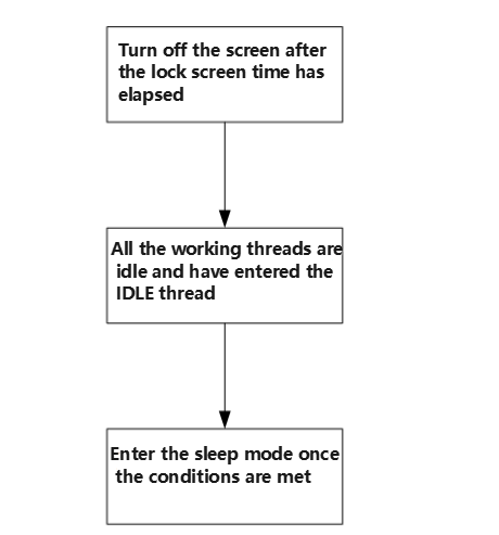
Figure 4.1 Screen‑off flow
4.5.2 HPSYS Wake‑Up
HPSYS can be woken by LPTIM, RTC, BLE MAC (LCPU only), Mailbox (other CPU), or any pin in DeepSleep. For example, press a button to wake HPSYS.
For button wake to turn the screen on, see Figure 4.2. After the screen turns on, a new screen‑off cycle begins. A wake‑up flow triggered by a smartphone app “setting” event is shown in Figure 4.3; after handling the request, the IDLE thread can immediately re‑enter sleep.
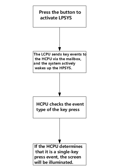
Figure 4.2 Button wake and screen‑off cycle
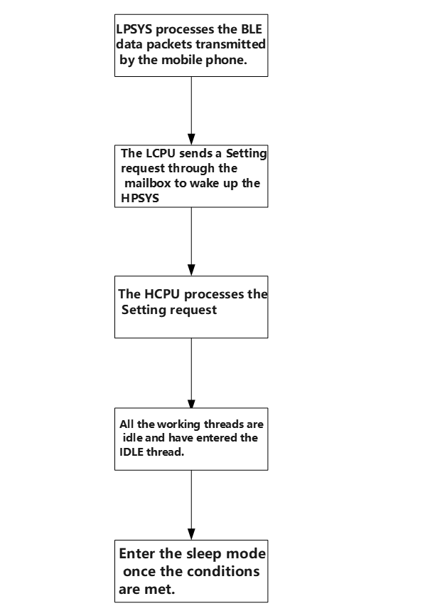
Figure 4.3 Wake‑up flow on phone Setting event
Context retention in DEEPSLEEP/STANDBY:
HCPU: In DEEPSLEEP, all RAM retained; restore directly from RAM after wake‑up.
LCPU: Keeps all RAM powered; saves CPU registers/context in RAM; restores directly from RAM on wake‑up.
4.6 Log Interpretation
HCPU and LCPU print logs via console. After enabling low‑power debug in Section 2.1, search the following keywords to analyze flows.
Table 4‑3: Log keywords
Log |
Meaning |
|---|---|
gui_suspend |
Screen off |
gui_resume |
Screen on |
[pm]S: mode,gtime |
Enter sleep; mode=2 means LIGHT, 4 means STANDBY; gtime unit is 32768 Hz |
[pm]W: gtime |
Exit sleep; gtime unit is 32768 Hz |
[pm]WSR:0xXXX |
Wake‑up reason (decode by register bitfields) |
gtime is synchronized between HCPU and LCPU. Example: sleep at 2136602 and wake at 2142330 → sleep_time=(2142330-2136602)/32768=175 ms. If WSR=0x200, wake‑up was by LPSYS mailbox interrupt. See the datasheet for bit meanings.
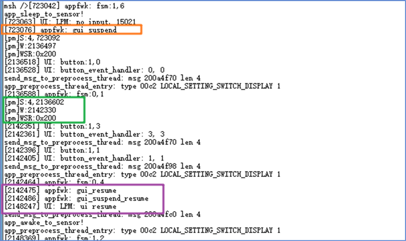
Figure 4.4 Low‑power log example
HPSYS WSR bits
Bit |
Description |
|---|---|
[0] |
RTC wake‑up |
[1] |
GPIO1 wake‑up |
[2] |
LPTIM1 wake‑up |
[3] |
PMUC wake‑up |
[6] |
LPSYS manual wake‑up HPSYS |
[7] |
LPSYS wake HPSYS via Mailbox |
[8] |
PIN0 wake‑up |
[9] |
PIN1 wake‑up |
[10] |
PIN2 wake‑up |
[11] |
PIN3 wake‑up |
[18] |
PIN10 wake‑up |
[19] |
PIN11 wake‑up |
[20] |
PIN12 wake‑up |
[21] |
PIN13 wake‑up |
[22] |
PIN14 wake‑up |
[23] |
PIN15 wake‑up |
[24] |
PIN16 wake‑up |
[25] |
PIN17 wake‑up |
[26] |
PIN18 wake‑up |
[27] |
PIN19 wake‑up |
[28] |
PIN20 wake‑up |
Table 4‑4: 52 series HPSYS wake‑up PIN mapping (partial)
Wake |
PIN |
|---|---|
PIN0 |
PA24 |
PIN1 |
PA25 |
PIN10 |
PA34 |
PIN11 |
PA35 |
PIN19 |
PA43 |
4.7 Common Issues Analysis
Since SWD cannot connect in sleep, use UART console logs to analyze issues.
4.7.1 Whether Sleep Was Entered
Likely HPSYS slept if any of:
SWD cannot connect
HCPU console no response
HCPU logs show “S: mode, gtime”
Likely LPSYS slept if any of:
LCPU console no response
LCPU logs show “S: mode, gtime”
Ensure the finsh shell option is enabled in LCPU Command shell.
You can also check chip power pins to determine current low‑power mode:
HPSYS active/sleep/deepsleep:
LDO1_VOUT≈ 1.1 V; HPSYS standby:LDO1_VOUTgradually drops to 0 V.LPSYS active/sleep/deepsleep:
LDO2_VOUTorBUCK2_VOUT≈ 0.9 V; LPSYS standby: the voltage gradually drops to 0 V.Hibernate:
LDO1_VOUT/LDO2_VOUT/BUCK2_VOUT/VDD_RETall drop to 0 V.
4.7.2 Why Sleep Didn’t Happen
Sleep entry conditions
For applications, sleep/work switching is transparently controlled by the lowest priority IDLE thread: when all higher‑priority threads are idle, IDLE runs and checks if all the following are met before entering sleep:
Sleep not forbidden (no outstanding
rt_pm_request(PM_SLEEP_MODE_IDLE))The soonest OS timer expiration > threshold (default 100 ms)
No wake condition currently satisfied (e.g., enabled wake source not active)
Data sent to the other core has been consumed (no unread data in IPC queues)
Timed wake configuration before sleep
Before sleep, configure LPTIM to interrupt at the soonest OS timer expiration so the timer callback fires on time during sleep. Example: if the next timer expires in 200 ms, set LPTIM to interrupt in 200 ms.
Forbid/release sleep APIs
Apps can explicitly suppress sleep in critical sections; the driver framework also suppresses sleep while peripherals are active to avoid sleeping during interrupt operations:
// Forbid sleep until release
rt_pm_request(PM_SLEEP_MODE_IDLE);
// ... critical section/peripheral operations ...
rt_pm_release(PM_SLEEP_MODE_IDLE);
Timer thresholds and policy
Refer to Power Management configuration for enabling low‑power support and selecting policies to enter different low‑power modes. The current default policy is:
Default policy example:
static const pm_policy_t default_pm_policy[] =
{
    {15, PM_SLEEP_MODE_LIGHT},                  // Idle > 15 ms → Light sleep
#ifdef PM_STANDBY_ENABLE
    {10000, PM_SLEEP_MODE_STANDBY},             // Idle > 10 s → Standby
#endif /* PM_STANDBY_ENABLE */
};
Common checks (HCPU/LCPU similar):
Enable PM and verify macros:
#define RT_USING_PM 1
#define BSP_USING_PM 1          // Enable low‑power
#define PM_DEEP_ENABLE 1        // Use Deep low‑power
#define BSP_PM_DEBUG 1          // Enable low‑power debug logs
Confirm CPU is idle and in the idle thread:
Use finsh
list_threadto check threads; excepttshellandtidleready, others should be suspend, otherwise IDLE cannot run.
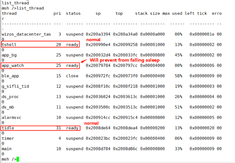
Figure 4.6 Output of list_thread
Confirm sleep is not forbidden:
In console, run
pm_dump. If “Idle Mode Counter” > 0, some module calledrt_pm_request(PM_SLEEP_MODE_IDLE)to forbid sleep; callrt_pm_release(PM_SLEEP_MODE_IDLE)to release.
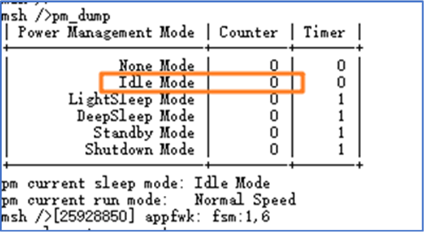
Figure 4.7 Output of pm_dump
Confirm OS timer expirations exceed the sleep threshold: In console, run
list_timerto show created timers. Compare the timeout of timers with flagactivatedagainst the sleep threshold; if smaller, that timer prevents sleep. Timeout unit is ms.
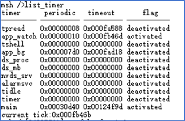
Figure 4.8 Output of list_timer
Default thresholds: HPSYS sleep threshold 100 ms; LPSYS sleep threshold 10 ms.
RT_WEAK const pm_policy_t pm_policy[] =
{
#ifdef PM_STANDBY_ENABLE
#ifdef SOC_BF0_HCPU
    {100, PM_SLEEP_MODE_STANDBY}, // HCPU: no timer wake within 100 ms → Standby
#else
    {10, PM_SLEEP_MODE_STANDBY},  // LCPU: no timer wake within 10 ms → Standby
#endif /* SOC_BF0_HCPU */
#elif defined(PM_DEEP_ENABLE)
#ifdef SOC_BF0_HCPU
    {100, PM_SLEEP_MODE_DEEP},    // HCPU: no timer wake within 100 ms → Deep
#else
    {10, PM_SLEEP_MODE_DEEP},     // LCPU: no timer wake within 10 ms → Deep
#endif /* SOC_BF0_HCPU */
#else
#ifdef SOC_BF0_HCPU
    {100, PM_SLEEP_MODE_LIGHT},
#else
}
If HCPU code uses a 90 ms periodic delay, the system will never enter sleep:
while (1)
{
    rt_thread_delay(90); // 90ms delay
}
Differences between delay functions:
HAL layer (no thread switch during delay):
HAL_Delay(10);     // 10ms
HAL_Delay_us(10);  // 10us
RT‑Thread interface (switches to other threads; may trigger idle→sleep):
rt_thread_delay(100); // 100ms
Ensure no pending wake‑up sources:
Read registers via console commands to check
WER/WSR:
52 series WSR addresses:
regop unlock 0000
regop read 40040024 1   # LPSYS WSR
regop read 500c0024 1   # HPSYS WSR
You can also use Jlink/SifliUsartServer to read registers or print via logs:
rt_kprintf("wsr:0x%x,wer:0x%x,\n", hwp_hpsys_aon->WSR, hwp_hpsys_aon->WER); // hcpu
rt_kprintf("wsr:0x%x,wer:0x%x,\n", hwp_lpsys_aon->WSR, hwp_lpsys_aon->WER); // lcpu
Common issue: wake‑up pin level misconfigured (e.g., configured for low‑level wake‑up but the pin remains low).
Ensure data sent to the other core has been consumed:
Use Ozone, memory dump with trace32, or log
ipc_ctxqueueread_idx_mirror/write_idx_mirror; inequality indicates unread data that blocks sleep.
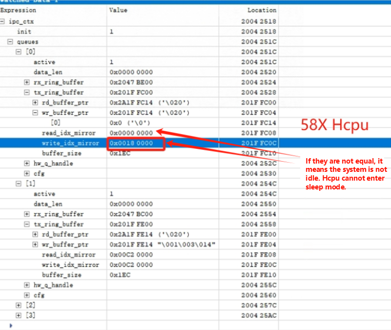
Figure 4.9 Non‑empty ring buffer
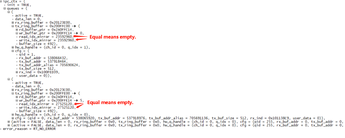
Figure 4.10 Empty ring buffer
Print activation queue index:
for (i = 0; i < IPC_LOGICAL_QUEUE_NUM; i++)
{
    if (ipc_ctx.queues[i].active == true)
    {
        if (ipc_ctx.queues[i].rx_ring_buffer && ipc_ctx.queues[i].tx_ring_buffer)
        {
            LOG_I("ipc_ctx.queues[%d].tx read_idx_mirror=0x%x, write_idx_mirror=0x%x\n",
                  i,
                  ipc_ctx.queues[i].tx_ring_buffer->read_idx_mirror,
                  ipc_ctx.queues[i].tx_ring_buffer->write_idx_mirror);
        }
    }
}
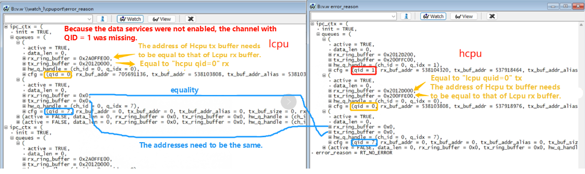
Figure 4.11 Example: LCPU data service disabled causing missing channel
5 Power Optimization Methods
5.1 Standby Leakage Analysis
When both HPSYS and LPSYS are in sleep, focus on system power optimization:
Remove detachable components (display, sensors, charging IC) and measure the minimum system current.
Misconfigured software IO levels can cause voltage differences/floating leakage.
On‑chip PSRAM/Flash and external NAND/Flash/eMMC may not have entered sleep.
If hardware allows measuring current per rail, identify the leaking rail (VSYS/ VLDO2/ VLDO3/ VDD_SIP/ VDDIOA) to narrow the scope.
5.1.1 Peripheral Leakage
Common causes:
Board‑level components are not powered off.
Board‑level components are powered off, but chip pin configuration causes back‑powering from the chip pins.
For case 2), avoid: driving high or enabling pull‑up on pins connected to powered‑off devices. Recommended pin settings for common peripherals in active/sleep are below (no change needed if external circuits stay powered; switch to low‑power configuration if external circuits are powered off).
Table 5‑1: Recommended Pin Settings
Peripheral |
Pin |
Dir |
Active |
Sleep (external on) |
Sleep (external off) |
|---|---|---|---|---|---|
PSRAM |
PSRAM_CLK |
O |
Digital out |
Digital out |
GPIO mode output low |
PSRAM |
PSRAM_CLKB |
O |
Digital out |
Digital out |
GPIO mode output low |
PSRAM |
PSRAM_CS |
O |
Digital out |
Digital out |
GPIO mode output low |
PSRAM |
PSRAM_DM0 |
O |
Digital out |
Digital out |
GPIO mode output low |
PSRAM |
PSRAM_DM1 |
O |
Digital out |
Digital out |
GPIO mode output low |
PSRAM |
PSRAM_DQS0 |
I/O |
Digital in‑pd |
Digital in‑pd |
Digital in‑pd |
PSRAM |
PSRAM_DQS1 |
I/O |
Digital in‑pd |
Digital in‑pd |
Digital in‑pd |
PSRAM |
PSRAM_DQx |
I/O |
Digital in‑pd |
Digital in‑pd |
Digital in‑pd |
QSPI |
QSPIx_CLK |
O |
Digital out |
Digital out |
GPIO mode output low |
QSPI |
QSPIx_CS |
O |
Digital out |
Digital out |
GPIO mode output low |
QSPI |
QSPIx_DIO0 |
I/O |
Digital in‑pd |
Digital in‑pd |
Digital in‑pd |
QSPI |
QSPIx_DIO1 |
I/O |
Digital in‑pd |
Digital in‑pd |
Digital in‑pd |
QSPI |
QSPIx_DIO2 |
I/O |
Digital in‑pu |
Digital in‑pu |
Digital in‑pd |
QSPI |
QSPIx_DIO3 |
I/O |
Digital in‑pu |
Digital in‑pu |
Digital in‑pd |
QSPI |
QSPIx_DIO4 |
I/O |
Digital in‑pd |
Digital in‑pd |
Digital in‑pd |
QSPI |
QSPIx_DIO5 |
I/O |
Digital in‑pd |
Digital in‑pd |
Digital in‑pd |
QSPI |
QSPIx_DIO6 |
I/O |
Digital in‑pu |
Digital in‑pu |
Digital in‑pd |
QSPI |
QSPIx_DIO7 |
I/O |
Digital in‑pu |
Digital in‑pu |
Digital in‑pd |
USART |
USARTx_RXD |
I |
Digital in‑pu |
Digital in‑pu |
Digital in‑pd |
USART |
USARTx_TXD |
O |
Digital out |
Digital out |
Digital out |
USART |
USARTx_CTS |
I |
Digital in‑pu |
Digital in‑pu |
Digital in‑pd |
USART |
USARTx_RTS |
O |
Digital out |
Digital out |
Digital out |
I2C |
I2Cx_SCL |
I/O |
Digital in |
Digital in |
Digital in‑pd |
I2C |
I2Cx_SDA |
I/O |
Digital in |
Digital in |
Digital in‑pd |
SPI M |
SPIx_CLK |
O |
Digital out |
Digital out |
GPIO mode output low |
SPI M |
SPIx_CS |
O |
Digital out |
Digital out |
GPIO mode output low |
SPI M |
SPIx_DI |
I |
Digital in‑pd |
Digital in‑pd |
Digital in‑pd |
SPI M |
SPIx_DO |
O |
Digital out |
Digital out |
GPIO mode output low |
SPI M |
SPIx_DIO |
I/O |
Digital in‑pd |
Digital in‑pd |
Digital in‑pd |
LCDC SPI |
LCDCx_SPI_CS |
O |
Digital out |
Digital out |
GPIO mode input pull‑down |
LCDC SPI |
LCDCx_SPI_CLK |
O |
Digital out |
Digital out |
GPIO mode input pull‑down |
LCDC SPI |
LCDCx_SPI_DIO0 |
I/O |
Digital in‑pd |
Digital in‑pd |
GPIO mode input pull‑down |
LCDC SPI |
LCDCx_SPI_DIO1 |
O |
Digital out |
Digital out |
GPIO mode input pull‑down |
LCDC SPI |
LCDCx_SPI_DIO2 |
O |
Digital out |
Digital out |
GPIO mode input pull‑down |
LCDC SPI |
LCDCx_SPI_DIO3 |
O |
Digital out |
Digital out |
GPIO mode input pull‑down |
LCDC SPI |
LCDCx_SPI_RSTB |
O |
Digital out |
Digital out |
GPIO output low |
LCDC SPI |
LCDCx_SPI_TE |
I |
Digital in |
Digital in |
GPIO mode input pull‑down |
SDIO |
SD_CLK |
O |
Digital out |
Digital out |
GPIO mode output low |
SDIO |
SD_CMD |
I/O |
Digital in‑pu |
Digital in‑pu |
Digital in‑pd |
SDIO |
SD_DIOx |
I/O |
Digital in‑pu |
Digital in‑pu |
Digital in‑pd |
I2S |
I2S1_BCK |
O |
Digital out |
Digital out |
GPIO mode output low |
I2S |
I2S1_LRCK |
O |
Digital out |
Digital out |
GPIO mode output low |
I2S |
I2S1_SDI |
I |
Digital in‑pd |
Digital in‑pd |
Digital in‑pd |
I2S |
I2S2_BCK |
O |
Digital out |
Digital out |
GPIO mode output low |
I2S |
I2S2_LRCK |
O |
Digital out |
Digital out |
GPIO mode output low |
I2S |
I2S2_SDI |
I |
Digital in‑pd |
Digital in‑pd |
Digital in‑pd |
I2S |
I2S2_SDO |
O |
Digital out |
Digital out |
GPIO mode output low |
PDM |
PDM_CLK |
O |
Digital out |
Digital out |
GPIO mode output low |
PDM |
PDM_DATA |
I |
Digital in‑pd |
Digital in‑pd |
Digital in‑pd |
GPTIM Out |
GPTIMx_CHx |
O |
Digital out |
Digital out |
GPIO mode output low |
GPTIM In |
GPTIMx_CHx |
I |
Digital in‑pd |
Digital in‑pd |
Digital in‑pd |
GPTIM |
GPTIMx_ETR |
I |
Digital in‑pd |
Digital in‑pd |
Digital in‑pd |
GPIO In |
GPIO |
I |
Digital in |
Digital in |
GPIO output low or digital in‑pd |
GPIO Out |
GPIO |
O |
Digital out |
Digital out |
GPIO mode output low |
5.1.2 On‑Chip IO Internal Leakage
Common patterns (see FAQ 8.7/8.8):
Input pins floating (peer device powered off equals floating), causing undefined levels.
IO output levels mismatch with internal/external pull‑ups or pull‑downs.
Below shows the pin internal structure (functional blocks: DS/OE/O/IE/PE/PS, etc.).
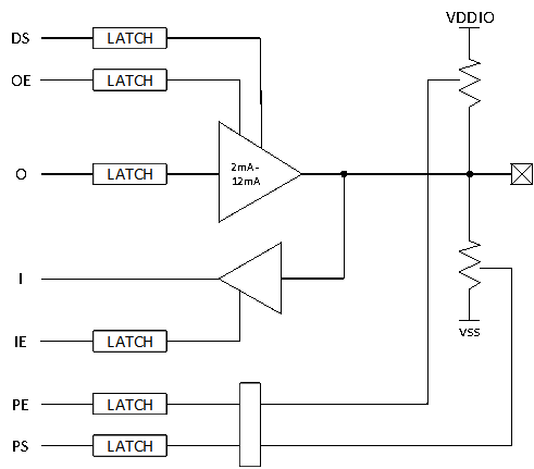
Figure 5.1 Pin internal structure
5.1.3 On‑chip/External Memory Leakage
PSRAM half‑sleep entry/exit example:
void BSP_Power_Up(bool is_deep_sleep)
{
#ifdef SOC_BF0_HCPU
    if (!is_deep_sleep)
    {
#if defined(BSP_USING_PSRAM1)
        rt_psram_exit_low_power("psram1"); // exit half_sleep
#endif
    }
    // ...
}

void BSP_IO_Power_Down(int coreid, bool is_deep_sleep)
{
#ifdef SOC_BF0_HCPU
    if (coreid == CORE_ID_HCPU)
    {
#if defined(BSP_USING_PSRAM1)
        rt_psram_enter_low_power("psram1");  // enter half_sleep
#endif
    }
#else
    // ...
#endif
}
NOR Flash power‑off and Deep Sleep example:
HAL_RAM_RET_CODE_SECT(BSP_PowerDownCustom, void BSP_PowerDownCustom(int coreid, bool is_deep_sleep))
{
#ifdef SOC_BF0_HCPU
#ifdef BSP_USING_NOR_FLASH2
    HAL_PMU_ConfigPeriLdo(PMU_PERI_LDO2_3V3, false, true); // turn off NOR flash power

    HAL_PIN_Set(PAD_PA16, GPIO_A16, PIN_PULLDOWN, 1); // after power off, set IO to pull‑down
    HAL_PIN_Set(PAD_PA12, GPIO_A12, PIN_PULLDOWN, 1);
    HAL_PIN_Set(PAD_PA15, GPIO_A15, PIN_PULLDOWN, 1);
    HAL_PIN_Set(PAD_PA13, GPIO_A13, PIN_PULLDOWN, 1);
    HAL_PIN_Set(PAD_PA14, GPIO_A14, PIN_PULLDOWN, 1);
    HAL_PIN_Set(PAD_PA17, GPIO_A17, PIN_PULLDOWN, 1);

    HAL_PIN_Set(PAD_PA35, GPIO_A35, PIN_PULLDOWN, 1);
    HAL_PIN_Set(PAD_PA36, GPIO_A36, PIN_PULLDOWN, 1);
#elif defined(BSP_USING_NOR_FLASH1)
    FLASH_HandleTypeDef *flash_handle;
    flash_handle = (FLASH_HandleTypeDef *)rt_flash_get_handle_by_addr(MPI1_MEM_BASE);
    HAL_FLASH_DEEP_PWRDOWN(flash_handle); // NOR flash enters deep sleep; IO state unchanged
    HAL_Delay_us(3);
#endif /* BSP_USING_NOR_FLASH2 */
#else
    { ; }
#endif
}

HAL_RAM_RET_CODE_SECT(BSP_PowerUpCustom, void BSP_PowerUpCustom(bool is_deep_sleep))
{
#ifdef SOC_BF0_HCPU
    if (!is_deep_sleep)
    {
#ifdef BSP_USING_NOR_FLASH2
        HAL_PIN_Set(PAD_PA16, MPI2_CLK,  PIN_NOPULL,   1); // restore IO to working state before power on
        HAL_PIN_Set(PAD_PA12, MPI2_CS,   PIN_NOPULL,   1);
        HAL_PIN_Set(PAD_PA15, MPI2_DIO0, PIN_PULLDOWN, 1);
        HAL_PIN_Set(PAD_PA13, MPI2_DIO1, PIN_PULLDOWN, 1);
        HAL_PIN_Set(PAD_PA14, MPI2_DIO2, PIN_PULLUP,   1);
        HAL_PIN_Set(PAD_PA17, MPI2_DIO3, PIN_PULLUP,   1);

        HAL_PIN_Set(PAD_PA35, GPIO_A35, PIN_PULLUP, 1);
        HAL_PIN_Set(PAD_PA36, GPIO_A36, PIN_PULLUP, 1);

        HAL_PMU_ConfigPeriLdo(PMU_PERI_LDO2_3V3, true, true); // turn on NOR flash power
        BSP_Flash_hw2_init(); // reinitialize NOR flash after power cycling
#elif defined(BSP_USING_NOR_FLASH1)
        FLASH_HandleTypeDef *flash_handle;
        flash_handle = (FLASH_HandleTypeDef *)rt_flash_get_handle_by_addr(MPI1_MEM_BASE);
        HAL_FLASH_RELEASE_DPD(flash_handle); // exit deep sleep
        HAL_Delay_us(20); // delay per datasheet tRES1
#endif
    }
    else if (PM_STANDBY_BOOT == SystemPowerOnModeGet())
    {
    }
#elif defined(SOC_BF0_LCPU)
    { ; }
#endif
}
Note: When running XIP from NOR flash, code controlling NOR sleep/wake must be placed in RAM (HAL_RAM_RET_CODE_SECT).
5.2 Code Implementation
Pin configuration code resides in the board’s pinmux.c and bsp_power.c. Implement BSP_PIN_Init, BSP_Power_Up, BSP_IO_Power_Down per IO definitions and hardware.
5.2.1 Pin Configuration in Active State
BSP_PIN_Init runs once on cold boot and after STANDBY wake‑up. Set functional modes and IO directions for active state here. For example, configure PB46 as USART3_RX with digital input pull‑up:
HAL_PIN_Set(PAD_PB46, USART3_RXD, PIN_PULLUP, 0);
For output IOs, configuring only PIN_NOPULL without setting a GPIO output leaves the pin in default input state, potentially causing floating leakage. Set an explicit output level, e.g.:
HAL_PIN_Set(PAD_PA35, GPIO_A35, PIN_NOPULL, 1);
// Then configure as explicit high/low output, or HAL_GPIO_DeInit to restore input when needed
5.2.2 Pin Configuration in Sleep State
In bsp_power.c, implement the following virtual functions to dynamically switch pin settings when entering/exiting sleep:
Table 5‑2: Pin Configuration APIs for Sleep State
Function |
Description |
|---|---|
BSP_IO_Power_Down |
Executed before entering sleep |
BSP_Power_Up |
Executed after wake‑up (STANDBY after |
BSP_TP_PowerDown |
Executed after screen off |
BSP_TP_PowerUp |
Executed before screen on |
BSP_LCD_PowerDown |
Executed after screen off |
BSP_LCD_PowerUp |
Executed before screen on |
If board‑level power control should align with sleep, you can power off components and adjust pins in BSP_IO_Power_Down, then reverse in BSP_Power_Up. This is coarse‑grained: e.g., after screen‑off, HPSYS may enter sleep later, and keeping LCD powered until then wastes energy; or when HPSYS wakes to run tasks without needing the screen, powering the screen in BSP_Power_Up also wastes energy. To refine control, handle display/touch power‑down in BSP_TP_PowerDown and BSP_LCD_PowerDown right after screen‑off, and call them again in BSP_Power_Up to keep pins in power‑down state until screen‑on. If screen‑on conditions are met, the system calls BSP_TP_PowerUp/BSP_LCD_PowerUp before lighting the screen to restore power and active pin settings.
Call order and coreid notes:
void BSP_IO_Power_Down(int coreid, bool is_deep_sleep)is called twice before HCPU sleeps:First with
coreid=CORE_ID_LCPU: before revoking LCPU wake requests, to close pins of LCPU peripherals used by HCPU. After revocation LCPU may enter low‑power and HCPU cannot access LCPU domain registers.Second with
coreid=CORE_ID_HCPU: right before HCPU sleep, to close pins used by HCPU itself.
In the LCPU project, this function is called once before LCPU sleeps to close pins used by LCPU.
Low‑power pin configurations differ per peripheral. Generally disable pull‑ups/downs to avoid leakage loops; output levels depend on board design and external device power state.
5.3 Sleep Flow
It is recommended to use DEEPSLEEP (sleep mode). In this mode all RAM data and hardware configurations are retained, wake‑up time back to active is shorter, and IO levels remain as in active state. Peripherals stop in sleep; CPU can only be woken by limited sources: GPIO interrupt, RTC interrupt, LPTIM interrupt, and inter‑core communication interrupt.
• HCPU sleep/wake (simplified):
Enter sifli_deep_handler(); without peripheral SUSPEND/RESUME and context restore, wake‑up is faster:
sifli_sleep → log [pm]S:3,11620140 → sifli_deep_handler → BSP_IO_Power_Down → WFI enter deep → timer/IO wake‑up → continue after returning from WFI → BSP_Power_Up → logs [pm]W:11620520, [pm]WSR:0x80.
Note: LCPU code is not open for modification on 52 series.
5.4 Hibernate Power‑Off Leakage Analysis
5.4.1 Hibernate Power‑Off Flow
Enter Hibernate: call HAL_PMU_EnterHibernate(). Before sleep, configure PMU wake‑up pins and levels for Hibernate. For 52 series, three internal LDOs exist; consider turning off unused LDOs via HAL_PMU_ConfigPeriLdo per hardware.
Hibernate wake‑up: press the wake‑up pin to wake. Use PM_HIBERNATE_BOOT == SystemPowerOnModeGet() to determine hibernate boot, and combine with button duration to decide whether to power on.
5.4.2 Hibernate Power‑Off Configuration
Before entering Hibernate:
Call
HAL_PMU_EnterHibernate().Configure PMU wake‑up pins and levels to ensure wake‑up.
58/56/52 series: PMU provides pull‑up/down in Hibernate (
hwp_rtc->PAWK1R/PAWK2R); configure viaHAL_PIN_Set.hwp_pmuc->WKUP_CNTsets external signal duration thresholds (58/56/52 series only).
– 52 series: Three internal LDOs (PMU_PERI_LDO_1V8/PMU_PERI_LDO2_3V3/PMU_PERI_LDO3_3V3); consider turning them off per hardware.
Example:
rt_kprintf("SF32LB52X entry_hibernate\n");
HAL_PMU_SelectWakeupPin(0, HAL_HPAON_QueryWakeupPin(hwp_gpio1, BSP_KEY1_PIN)); // select PA34 → wake_pin0
HAL_PMU_EnablePinWakeup(0, AON_PIN_MODE_HIGH);                                 // enable wake_pin0
hwp_pmuc->WKUP_CNT = 0x50005; // 31-16bit: PIN1 wake CNT, 15-0bit: PIN0 wake CNT
rt_kprintf("SF32LB52X CR:0x%x,WER:0x%x\n", hwp_pmuc->CR, hwp_pmuc->WER);

HAL_PIN_Set(PAD_PA24, GPIO_A24, PIN_PULLDOWN, 1); // #WKUP_PIN0
HAL_PIN_Set(PAD_PA25, GPIO_A25, PIN_PULLDOWN, 1); // #WKUP_PIN1
HAL_PIN_Set(PAD_PA26, GPIO_A26, PIN_PULLDOWN, 1); // #WKUP_PIN2
HAL_PIN_Set(PAD_PA27, GPIO_A27, PIN_PULLDOWN, 1); // #WKUP_PIN3

HAL_PIN_Set(PAD_PA34, GPIO_A34, PIN_PULLDOWN, 1); // #WKUP_PIN10
HAL_PIN_Set(PAD_PA35, GPIO_A35, PIN_PULLDOWN, 1); // #WKUP_PIN11
HAL_PIN_Set(PAD_PA36, GPIO_A36, PIN_PULLDOWN, 1); // #WKUP_PIN12
HAL_PIN_Set(PAD_PA37, GPIO_A37, PIN_PULLDOWN, 1); // #WKUP_PIN13
HAL_PIN_Set(PAD_PA38, GPIO_A38, PIN_PULLDOWN, 1); // #WKUP_PIN14
HAL_PIN_Set(PAD_PA39, GPIO_A39, PIN_PULLDOWN, 1); // #WKUP_PIN15
HAL_PIN_Set(PAD_PA40, GPIO_A40, PIN_PULLDOWN, 1); // #WKUP_PIN16
HAL_PIN_Set(PAD_PA41, GPIO_A41, PIN_PULLDOWN, 1); // #WKUP_PIN17
HAL_PIN_Set(PAD_PA42, GPIO_A42, PIN_PULLDOWN, 1); // #WKUP_PIN18
HAL_PIN_Set(PAD_PA43, GPIO_A43, PIN_PULLDOWN, 1); // #WKUP_PIN19
HAL_PIN_Set(PAD_PA44, GPIO_A44, PIN_PULLDOWN, 1); // #WKUP_PIN20

rt_hw_interrupt_disable();
HAL_PMU_ConfigPeriLdo(PMU_PERI_LDO2_3V3, false, false);
HAL_PMU_ConfigPeriLdo(PMU_PERI_LDO3_3V3, false, false);
HAL_PMU_ConfigPeriLdo(PMU_PERI_LDO_1V8,  false, false);
HAL_PMU_EnterHibernate();
Notes:
58/56/52 series: Only two wake‑up sources (
pin0/pin1) are allowed at the same time; map viaHAL_PMU_SelectWakeupPin.
– 52 series: #WKUP_PIN4-9 (PA28-PA33) are multiplexed with ADC and no longer support wake‑up; disconnect external IO and use internal pull‑down (no handling needed in Hibernate, no leakage). Do not set pull‑ups via hwp_rtc->PAWK1R/PAWK2R to avoid leakage.
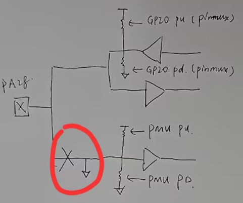
Figure 5.2 Handling of #WKUP_PIN4‑9 in 52 series Hibernate
Hibernate wake‑up detection:
if (PM_HIBERNATE_BOOT == SystemPowerOnModeGet())
{
    // Decide whether to power on based on button duration, etc.
}