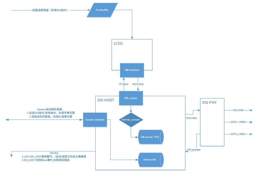
DSI
DSI (MIPI DSI) module supports 1-lane or 2-lane DSI screens, currently supporting bandwidth configurations of 240/288/336/384/480Mbps, based on MIPI protocol version V1.1 (55x does not support Video mode).
Supported Color Output Formats
RGB565 DSItransmission order: [G3~G5R0~R4][B0~B4G0~G2]RGB888 DSItransmission order: [R0~R7][G0~G7][B0~B7]RGB565_SWAP DSItransmission order (55X not supported): [B0~B4G0~G2][G3~G5R0~R4]
DSI module can work independently, but operating through LCDC encapsulated interface can achieve optimal performance.
Note
On 55x, DSI needs multiple operations to complete the entire screen refresh, refreshing 2N lines each time (N varies depending on refresh area size), until the entire screen refresh is completed
DSI Usage Example
Open DSI screen through LCDC interface, then draw a 100x100 rectangular area to LCD:
static LCDC_HandleTypeDef hlcdc_rm69090;


/*DSI LCD configuration*/
static const LCDC_InitTypeDef lcdc_int_cfg =
{
    .lcd_itf = LCDC_INTF_DSI,                              //LCDC output interface
    .freq = DSI_FREQ_288MHZ,                               //DSI clk lane frequency(DDR frequency)
    .color_mode = LCDC_PIXEL_FORMAT_RGB888,                //LCDC DBI output color format, should match with CmdCfg.ColorCoding below

    .cfg = {

        .dsi = {

            .Init = {
                .AutomaticClockLaneControl = DSI_AUTO_CLK_LANE_CTRL_DISABLE,        //Auto gate clock to save power
                .NumberOfLanes = DSI_TWO_DATA_LANES,                                //Numbers of data-lane
                .TXEscapeCkdiv = 0x2,                                               //Escape clk = lcdc_int_cfg_dsi.freq / 2 / 8 / TXEscapeCkdiv
            },

            .CmdCfg = {
                .VirtualChannelID      = 0,                             //Fixed 0,  DBI virtual channel id
                .CommandSize           = 0xFFFF,                        //Maximum write bytes of every partial write
                .TEAcknowledgeRequest  = DSI_TE_ACKNOWLEDGE_ENABLE,     //Open or Close TE
                .ColorCoding           = DSI_RGB888,                    //DSI-DBI input color format and DSI output format
            },

            .PhyTimings = { /*DSI PHY config */
                .ClockLaneHS2LPTime = 35,  /* The maximum time that the D-PHY clock lane takes to go from high-speed
                                              to low-power transmission                                              */
                .ClockLaneLP2HSTime = 35,  /* The maximum time that the D-PHY clock lane takes to go from low-power
                                              to high-speed transmission                                             */
                .DataLaneHS2LPTime = 35,   /* The maximum time that the D-PHY data lanes takes to go from high-speed
                                              to low-power transmission                                              */
                .DataLaneLP2HSTime = 35,   /* The maximum time that the D-PHY data lanes takes to go from low-power
                                              to high-speed transmission                                             */

                .DataLaneMaxReadTime = 0,  /* The maximum time required to perform a read command */
                .StopWaitTime = 10,        /* The minimum wait period to request a High-Speed transmission after the
                                              Stop state                                                             */
            },

            .HostTimeouts = {
                .TimeoutCkdiv = 1,                          //Timeout clk = lcdc_int_cfg_dsi.freq / 2 / 8 / TimeoutCkdiv
                .HighSpeedTransmissionTimeout = 0,
                .LowPowerReceptionTimeout = 0,
                .HighSpeedReadTimeout = 0,
                .LowPowerReadTimeout = 0,
                .HighSpeedWriteTimeout = 0,
                //.HighSpeedWritePrespMode = DSI_HS_PM_DISABLE,
                .LowPowerWriteTimeout = 0,
                .BTATimeout = 0,
            },


            .LPCmd = {
                .LPGenShortWriteNoP    = DSI_LP_GSW0P_ENABLE,     //Generic short write 0 parameter use LP mode
                .LPGenShortWriteOneP   = DSI_LP_GSW1P_ENABLE,     //Generic short write 1 parameter use LP mode
                .LPGenShortWriteTwoP   = DSI_LP_GSW2P_ENABLE,     //Generic short write 2 parameter use LP mode
                .LPGenShortReadNoP     = DSI_LP_GSR0P_ENABLE,     //Generic short read 0 parameter use LP mode
                .LPGenShortReadOneP    = DSI_LP_GSR1P_ENABLE,     //Generic short read 0 parameter use LP mode
                .LPGenShortReadTwoP    = DSI_LP_GSR2P_ENABLE,     //Generic short read 0 parameter use LP mode
                .LPGenLongWrite        = DSI_LP_GLW_ENABLE,       //Generic long write use LP mode
                .LPDcsShortWriteNoP    = DSI_LP_DSW0P_ENABLE,     //Dcs short write 0 parameter use LP mode
                .LPDcsShortWriteOneP   = DSI_LP_DSW1P_ENABLE,     //Dcs short write 1 parameter use LP mode
                .LPDcsShortReadNoP     = DSI_LP_DSR0P_ENABLE,     //Dcs short read 0 parameter use LP mode
                .LPDcsLongWrite        = DSI_LP_DLW_DISABLE,      //Dcs long write use HS mode
                .LPMaxReadPacket       = DSI_LP_MRDP_ENABLE,      //Maximum Read Packet Size
                .AcknowledgeRequest    = DSI_ACKNOWLEDGE_DISABLE, //Request acknowledge
            },


            .vsyn_delay_us = 1000,  //The delay during receive TE and send framebuffer. If TE was disable ignore it.
        },
    },
};


/**********************
 *   FUNCTIONS
 **********************/

__ROM_USED void LCDC1_IRQHandler(void)
{
    /* enter interrupt */
    ENTER_INTERRUPT();

    HAL_LCDC_IRQHandler(&hlcdc_rm69090);

    /* leave interrupt */
    LEAVE_INTERRUPT();
}


void HAL_LCDC_SendLayerDataCpltCbk(LCDC_HandleTypeDef *lcdc)
{
    LOG_I("Send layer buffer done.");
}

/*
    RM69090 initialization sequence
 */
static void RM69090_Init_Seq(LCDC_HandleTypeDef *hlcdc)
{
    ...

    //Sleep out
    HAL_LCDC_WriteU8Reg(hlcdc, 0x11, (uint8_t *)NULL, 0);

    /* Wait for 150ms */
    HAL_Delay(150);

    /* Display On */
    HAL_LCDC_WriteU8Reg(hlcdc, 0x29, (uint8_t *)NULL, 0);

    /* Wait for 150ms */
    HAL_Delay(150);

    ...
}


/*Set LCD receive area*/
void RM69090_SetRegion(LCDC_HandleTypeDef *hlcdc, uint16_t x0, uint16_t y0, uint16_t x1, uint16_t y1)
{
    uint8_t   parameter[4];

    parameter[0] = (x0) >> 8;
    parameter[1] = (x0) & 0xFF;
    parameter[2] = (x1) >> 8;
    parameter[3] = (x1) & 0xFF;
    HAL_LCDC_WriteU8Reg(hlcdc, 0x2a, parameter, 4);

    parameter[0] = (y0) >> 8;
    parameter[1] = (y0) & 0xFF;
    parameter[2] = (y1) >> 8;
    parameter[3] = (y1) & 0xFF;
    HAL_LCDC_WriteU8Reg(hlcdc, 0x2b, parameter, 4);
}


static void main(int argc, char **argv)
{
    uint8_t *p_framebuffer = (uint8_t *) 0x60020000;

    /*Turn on LCD board power supply*/
    Poweron_LCD_Board();


    memset(&hlcdc_rm69090, 0, sizeof(hlcdc_rm69090));

    hlcdc_rm69090.Instance = hwp_lcdc;

    /*Set background layer color*/
    hlcdc_rm69090.bg.r = 0;
    hlcdc_rm69090.bg.g = 0;
    hlcdc_rm69090.bg.b = 255;

    /*Set default layer configuration*/
    hlcdc_rm69090.Layer.layer_alpha_en = 0;
    hlcdc_rm69090.Layer.alpha = 255;
    hlcdc_rm69090.Layer.chroma_key_en = 0;

    memcpy(&hlcdc_rm69090.Init, &lcdc_int_cfg, sizeof(LCDC_InitTypeDef));

    /*Open DSI & LCDC */
    HAL_LCDC_Init(&hlcdc_rm69090);

    /*  Reset LCD by RESX pin */
    HAL_LCDC_ResetLCD(&hlcdc_rm69090, LCDC_RESX_NEG_PULSE, 20);
    /* Wait for 200ms */
    HAL_Delay(200);


    /*DSI LCD initial */
    RM69090_Init_Seq(&hlcdc_rm69090);

    {//Read LCD id

        uint32_t rd_data = 0;

        HAL_LCDC_ReadU8Reg(&hlcdc_rm69090, 0x04, (uint8_t *)&rd_data, 4);
        LOG_I("rm69090 id is %d",rd_data);
    }

    /*Disable layer compress*/
    HAL_LCDC_LayerSetCmpr(&hlcdc_rm69090, HAL_LCDC_LAYER_DEFAULT, 0);
    /*Set layer format RGB565*/
    HAL_LCDC_LayerSetFormat(&hlcdc_rm69090, HAL_LCDC_LAYER_DEFAULT,LCDC_PIXEL_FORMAT_RGB565);

    /*Fill framebuffer with single color*/
    memset(p_framebuffer, 0xE0, 100*100*2);

    /*Assign framebuffer  and area to layer*/
    HAL_LCDC_LayerSetData(&hlcdc_rm69090, HAL_LCDC_LAYER_DEFAULT, (uint8_t *)p_framebuffer, 100, 100, 199, 199);


    /*Set clip area of all LCDC layer*/
    HAL_LCDC_SetROIArea(&hlcdc_rm69090, 100, 100, 199, 199);

    /*Set LCD receive area */
    RM69090_SetRegion(&hlcdc_rm69090, 100, 100, 199, 199);

    /*Enable LCDC IRQ*/
    HAL_NVIC_SetPriority(LCDC_IRQ_NUM, 3, 0);
    HAL_NVIC_EnableIRQ(LCDC_IRQ_NUM);


    /*
        Start partial writing framebuffer,

       RM69090_SetRegion is the function of setting LCD receive area, and it was called during partial write DSI LCD
    */
    HAL_LCDC_DSI_StartPatialWrite(&hlcdc_rm69090, 0x2c, (SetRegion_cb_t)RM69090_SetRegion);

    /* Wait for 150ms */
    HAL_Delay(150);

   /*Writing framebuffer is done while LCDC_IRQHandler come*/

    /*Disable LCDC IRQ*/
    HAL_NVIC_DisableIRQ(LCDC_IRQ_NUM);

}