ADC Example
Source code path: example\hal\adc\multichannel
Supported Platforms
The example can run on the following development boards
sf32lb52-lcd_n16r8
Overview
Operating HAL functions for single-channel ADC or DMA six-channel sampling demonstration
Example Usage
Compilation and Programming
The demonstration code defaults to single-channel ADC sampling demonstration. If you want to run the DMA six-channel demonstration, please enable the macro in main.c under the project path:
#define BSP_GPADC_USING_DMA 1
Switch to the example project directory and run the scons command to compile:
scons –board=sf32lb52-lcd_n16r8 -j8
Switch to the example project/build_xx directory and run uart_download.bat, select the port as prompted to download:
build_sf32lb52-lcd_n16r8_hcpu\uart_download.bat
Uart Download
please input the serial port num:5
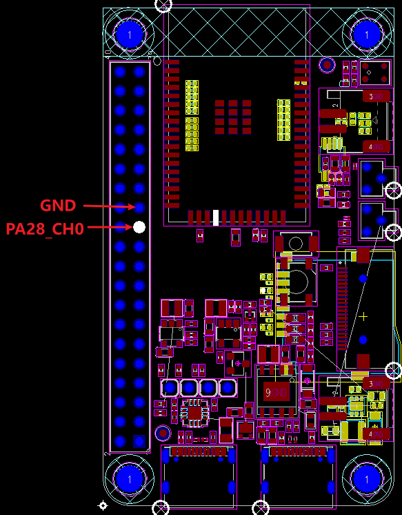
Hardware Connection
PA28 is the fixed output IO for ADC1 Channel 0 (DMA six-channel demonstration uses PA28-PA33, not marked here)
Example Output Results Display:
Single-channel ADC mode log output (PA28 input 2.5V):
    SFBL
    Serial:c2,Chip:4,Package:3,Rev:3  Reason:00000080
     \ | /
    - SiFli Corporation
     / | \     build on Nov  6 2024, 2.2.0 build 00000000
     2020 - 2022 Copyright by SiFli team
    mount /dev sucess
    [I/drv.rtc] PSCLR=0x80000100 DivAI=128 DivAF=0 B=256
    [I/drv.rtc] RTC use LXT RTC_CR=00000001
    [I/drv.rtc] Init RTC, wake = 0
    [I/drv.audprc] init 00 ADC_PATH_CFG0 0x606
    [I/drv.audprc] HAL_AUDPRC_Init res 0
    [I/drv.audcodec] HAL_AUDCODEC_Init res 0
    [32m][I/TOUCH] Regist touch screen driver, probe=1203c2d5 [0m]
    call par CFG1(35bb)
    fc 9, xtal 2000, pll 2050
    call par CFG1(35bb)
    fc 9, xtal 2000, pll 2050
    Start adc demo!
    ADC Get calibration res 0
    ADC reg value 3192 voltage 2519.12 mv
    adc demo end!
The log prints the value as the raw register value, and Voltage is the converted mV voltage
DMA six-channel mode log output (PA28 input 2.5V, PA29 connected to GND, other IOs based on board internal voltage):
   SFBL
   Serial:c2,Chip:4,Package:3,Rev:3  Reason:00000080
    \ | /
   - SiFli Corporation
    / | \     build on Nov  6 2024, 2.2.0 build 00000000
    2020 - 2022 Copyright by SiFli team
   mount /dev sucess
   [I/drv.rtc] PSCLR=0x80000100 DivAI=128 DivAF=0 B=256
   [I/drv.rtc] RTC use LXT RTC_CR=00000001
   [I/drv.rtc] Init RTC, wake = 0
   [I/drv.audprc] init 00 ADC_PATH_CFG0 0x606
   [I/drv.audprc] HAL_AUDPRC_Init res 0
   [I/drv.audcodec] HAL_AUDCODEC_Init res 0
   [32m][I/TOUCH] Regist touch screen driver, probe=1203c685 [0m]
   call par CFG1(35bb)
   fc 9, xtal 2000, pll 2050
   call par CFG1(35bb)
   fc 9, xtal 2000, pll 2050
   Start adc demo!
   ADC Get calibration res 0
   ADC reg value[0] 3199 voltage 2526.56 mv
   ADC reg value[1] 831 voltage 10.98 mv
   ADC reg value[2] 3950 voltage 3324.36 mv
   ADC reg value[3] 1757 voltage 994.69 mv
   ADC reg value[4] 1082 voltage 277.62 mv
   ADC reg value[5] 3951 voltage 3325.43 mv
   Loop 0 done ===
   adc demo end!
The log prints value[0] as the corresponding channel 0 raw register value, and Voltage is the converted mV voltage
ADC Configuration Flow
Set the corresponding ADC IO port (single-channel ADC mode)
    /* 52 chip default channel 0 is PA28, set PA28 to analog input mode, disable internal pull-up/pull-down */
    HAL_PIN_Set_Analog(PAD_PA28, 1);
Set the corresponding ADC IO ports (DMA six-channel mode)
    /* 52 chip demonstration uses channels 0-5, all configured as analog input mode, disable internal pull-up/pull-down */
    HAL_PIN_Set_Analog(PAD_PA28, 1);  /* channel 0 */
    HAL_PIN_Set_Analog(PAD_PA29, 1);
    HAL_PIN_Set_Analog(PAD_PA30, 1);
    HAL_PIN_Set_Analog(PAD_PA31, 1);
    HAL_PIN_Set_Analog(PAD_PA32, 1);
    HAL_PIN_Set_Analog(PAD_PA33, 1);  /* channel 5 */
Note:
ADC input ports are fixed IO ports, as shown in the following diagram:
52 chip ADC CH1-7 distribution, corresponding to software configured Channel0-6. The last channel CH8 (Channel 7) is internally connected to battery Vbat detection and not mapped to external IO
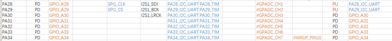
HAL_PIN_SetHAL_PIN_Set_Analoglast parameter is for hcpu/lcpu selection, 1: select hcpu, 0: select lcpu
Enable the corresponding ADC clock source (enabled by default in code, not mandatory here)
    /* 2, open adc clock source  */
    HAL_RCC_EnableModule(RCC_MOD_GPADC);
ADC initialization settings
ADC channel modification
   #define ADC_DEV_CHANNEL     0           /* Single-channel ADC mode ADC channel */
    /* 52 chip default channel 0 is PA28, set PA28 to analog input mode, disable internal pull-up/pull-down */
    HAL_PIN_Set_Analog(PAD_PA28, 1);
    /* Select which channels to sample with DMA  */
    /* set pinmux of channel 0 to analog input */
    HAL_PIN_Set_Analog(PAD_PA28, 1);  /* channel 0 */
    HAL_PIN_Set_Analog(PAD_PA29, 1);
    HAL_PIN_Set_Analog(PAD_PA30, 1);
    HAL_PIN_Set_Analog(PAD_PA31, 1);
    HAL_PIN_Set_Analog(PAD_PA32, 1);
    HAL_PIN_Set_Analog(PAD_PA33, 1);  /* channel 5 */
    /* ADC has 8 slots total, can be used to simultaneously sample 8-channel ADC. Channel 0 corresponds to slot0. To simultaneously sample which channels, enable the corresponding slots */
    ADC_ChanConf.Channel = 0; /* channel 0 */
    ADC_ChanConf.pchnl_sel = 0; /* channel 0 */
    ADC_ChanConf.slot_en = 1; /* Enable slot 0 to sample channel 0 */
    ADC_ChanConf.acc_num = 0;
    HAL_ADC_ConfigChannel(&hadc, &ADC_ChanConf);
ADC Calibration
To improve ADC accuracy, SiFli series chips undergo ADC calibration at the factory (calibration parameters are written to the chip’s internal OTP area). Different series have different calibration methods.
To ensure ADC accuracy, it needs to be called once every power-on. The following is the calibration function, which reads OTP parameters to calculate the slopeadc_vol_ratioand offsetadc_vol_offset:
static int utest_adc_calib(void)
After ADC sampling obtains the raw register value, call the function
example_adc_get_float_mvand calculate the final voltage value based on the calibrated slopeadc_vol_ratioand offsetadc_vol_offset.For 52 series chips, CH8 (Channel 7) is internally connected to Vbat through two equal voltage divider resistors. To get the Vbat value, conversion is needed. To reduce voltage divider resistor errors, the two resistors have been calibrated at the factory:
static float adc_vbat_factor = 2.01; /* Calibrate the two voltage divider resistors from 52 chip internal CH8 (Channel 7) to Vbat */
static void example_adc_vbat_fact_calib(uint32_t voltage, uint32_t reg)
{
    float vol_from_reg;

    // get voltage calculate by register data
    vol_from_reg = (reg - adc_vol_offset) * adc_vol_ratio / ADC_RATIO_ACCURATE;
    adc_vbat_factor = (float)voltage / vol_from_reg;
}
/* Method to convert CH8 (Channel 7) sampling to Vbat voltage value, refer to code in sifli_get_adc_value function */
    float fval = sifli_adc_get_float_mv(fave) * 10; // mv to 0.1mv based
    *value = (rt_uint32_t)fval;
    if (channel == 7)   // for 52x, channel fix used for vbat with 1/2 update(need calibrate)
        *value = (rt_uint32_t)(fval * adc_vbat_factor); /* Convert sampled actual ADC voltage to Vbat voltage value*/
Exception Diagnosis
ADC sampled voltage value is incorrect
Check if ADC hardware is connected correctly. ADC sampling channels are fixed IO ports and cannot be arbitrarily assigned. For which IO corresponds to CH0-7, refer to the chip manual.
ADC input voltage range is 0V - reference voltage (52 defaults to 3v3), cannot exceed the input range
Use debugging tools like Ozone or LightWork. After starting ADC sampling, connect online and check the corresponding register configuration status against the chip manual.
ADC accuracy is insufficient
Check if ADC calibration parameters are obtained and used
Check if voltage divider resistor accuracy meets requirements
Check if ADC reference voltage is stable and has excessive ripple (refer to ADC voltage reference chip manual for specifics)
Reference Documents
EH-SF32LB52X_Pin_config_V1.3.0_20231110.xlsx
DS0052-SF32LB52x-芯片技术规格书 V0p3.pdf
Update Log
Version |
Date |
Release Notes |
|---|---|---|
0.0.1 |
10/2024 |
Initial version |