
GPADC Button
Source path: example/misc/adc_button
Supported Platforms
sf32lb57-spi-hdk_n16r4
Overview
A GPADC button uses a resistor divider network to convert the state of multiple buttons into distinct voltage levels, then uses a single ADC channel to sample and identify which button was pressed. Compared with the traditional one-GPIO-per-button approach, it saves a significant number of pins: a single ADC channel plus one GPIO interrupt (used for wake-up) can support multiple buttons, making it well suited to pin-constrained scenarios.
This example demonstrates how to drive GPADC buttons using the SDK’s button library. When a button is pressed, the corresponding button number and action type are printed to the serial console.
Principle
Hardware Principle
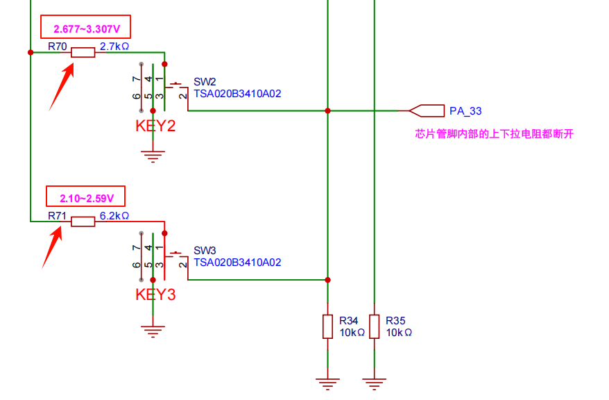
Each button is connected in series with a resistor of a different value, and all of them are tied to the same ADC pin. When different buttons are pressed, the divider ratio differs, so the ADC pin sees a unique and distinguishable voltage:
Button 1 pressed → ADC voltage = VCC × R1 / (R_pullup + R1)
Button 2 pressed → ADC voltage = VCC × R2 / (R_pullup + R2)
...
As long as the resistor values are chosen properly so that the voltage ranges of the buttons do not overlap, the button number can be looked up from the ADC sample value.
Software Detection Flow
Any button press → the shared GPIO generates an edge interrupt
The button library performs debouncing in a software timer (the
timerthread)Once debouncing passes, the pin is temporarily switched to analog function and the ADC is read once
The sampled voltage is compared against each button’s configured range; a match yields the button index
After the read, the pin is switched back to GPIO, the interrupt is re-enabled, and the application-registered callback is invoked
The voltage comparison logic (middleware/button/button.c):
/* The raw value read back from the ADC is in units of 0.1mV; convert to mV first */
read_arg.value /= 10;
for (i = 0; i < adc_btn_group_cfg->num; i++)
{
    if ((read_arg.value >= (adc_btn_cfg[i].voltage - adc_btn_cfg[i].volt_range))
            && (read_arg.value <= (adc_btn_cfg[i].voltage + adc_btn_cfg[i].volt_range)))
    {
        break;      /* Match, i is the button index */
    }
}
Therefore the VOLT and RANGE configuration items are both in units of mV, and the match condition is VOLT - RANGE ≤ measured voltage ≤ VOLT + RANGE.
Using the Example
menuconfig Configuration
sdk.py menuconfig --board=sf32lb57-spi-hdk_n16r4_hcpu
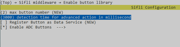
The long-press detection duration is controlled by BUTTON_ADV_ACTION_CHECK_DELAY (in ms), configured under SiFli Middleware -> Enable button library. This example sets it to 1000, meaning a press held longer than 1 second is treated as a long press.
Build and Flash
Switch to the example’s project directory and run the build:
scons --board=sf32lb57-spi-hdk_n16r4_hcpu -j8
Run build_sf32lb57-spi-hdk_n16r4_hcpu\uart_download.bat and select the port as prompted to flash:
build_sf32lb57-spi-hdk_n16r4_hcpu\uart_download.bat
Uart Download
please input the serial port num: 5
For details, see the build and flash documentation.
Adapting to New Hardware
When switching boards, calibrate the voltages as follows:
Compute from the schematic, or measure with a multimeter, the ADC pin voltage when each button is pressed
Use the midpoint of the range as
BUTTONx_VOLTUse the half-width of the range as
BUTTONx_RANGE, ensuring that the[VOLT-RANGE, VOLT+RANGE]intervals of adjacent buttons do not overlapSet
GROUP1_MAX_NUMaccording to the actual number of buttons, and setGROUP1_ADC_DEV_CHANNELandBSP_KEY1_PINaccording to the actual wiring
If you are unsure of the measured values, flash a build first. The log line adc control origin data ... Voltage ... prints the raw value of each sample (in units of 0.1mV; divide by 10 to get mV), which you can use to work backward to the configuration.
Example Output
After startup, short-press buttons 1, 2, and 3 in sequence, then long-press button 2:
ADC button ready, 3 keys. Press a key to see the log.
msh />
adc control origin data 3712, Voltage 30865
key 1 pressed
key 1 clicked
key 1 released
adc control origin data 3311, Voltage 26582
key 2 pressed
key 2 clicked
key 2 released
adc control origin data 2914, Voltage 22342
key 3 pressed
key 3 clicked
key 3 released
adc control origin data 3309, Voltage 26561
key 2 pressed
key 2 long pressed
key 2 released
Log interpretation:
adc control origin datais the raw ADC code value;Voltageis in units of 0.1mVButton 1: 30865 × 0.1mV = 3086mV, which falls within 2973 ± 150 = [2823, 3123] → index 0, prints
key 1Button 2: 26582 × 0.1mV = 2658mV, which falls within 2578 ± 150 = [2428, 2728] → index 1, prints
key 2Button 3: 22342 × 0.1mV = 2234mV, which falls within 2185 ± 150 = [2035, 2335] → index 2, prints
key 3Each press samples the ADC only once, before
BUTTON_PRESSED; the subsequent clicked / long pressed / released events reuse the same button index, so the voltage is not printed repeatedlyThe short-press sequence is
pressed → clicked → released; the long-press sequence ispressed → long pressed → released
Troubleshooting
Problem |
Possible Cause |
Solution |
|---|---|---|
Assertion at startup that |
|
Add |
|
The |
Check the board-level |
No response to button presses |
The interrupt GPIO is misconfigured, or |
Verify |
Prints |
The measured voltage does not fall within any button’s configured range |
Re-calibrate |
A button is recognized as an adjacent button |
The button voltage ranges overlap, or |
Reduce |
Long press does not trigger |
The long-press threshold is too large |
Reduce |
Abnormal ADC channel readings |
|
Verify the ADC channel the buttons are connected to on the schematic |
Revision History
Version |
Date |
Release Notes |
|---|---|---|
0.0.2 |
07/2026 |
Adapted to sf32lb57-spi-hdk_n16r4; rewrote example and documentation |
0.0.1 |
08/2025 |
Initial version |